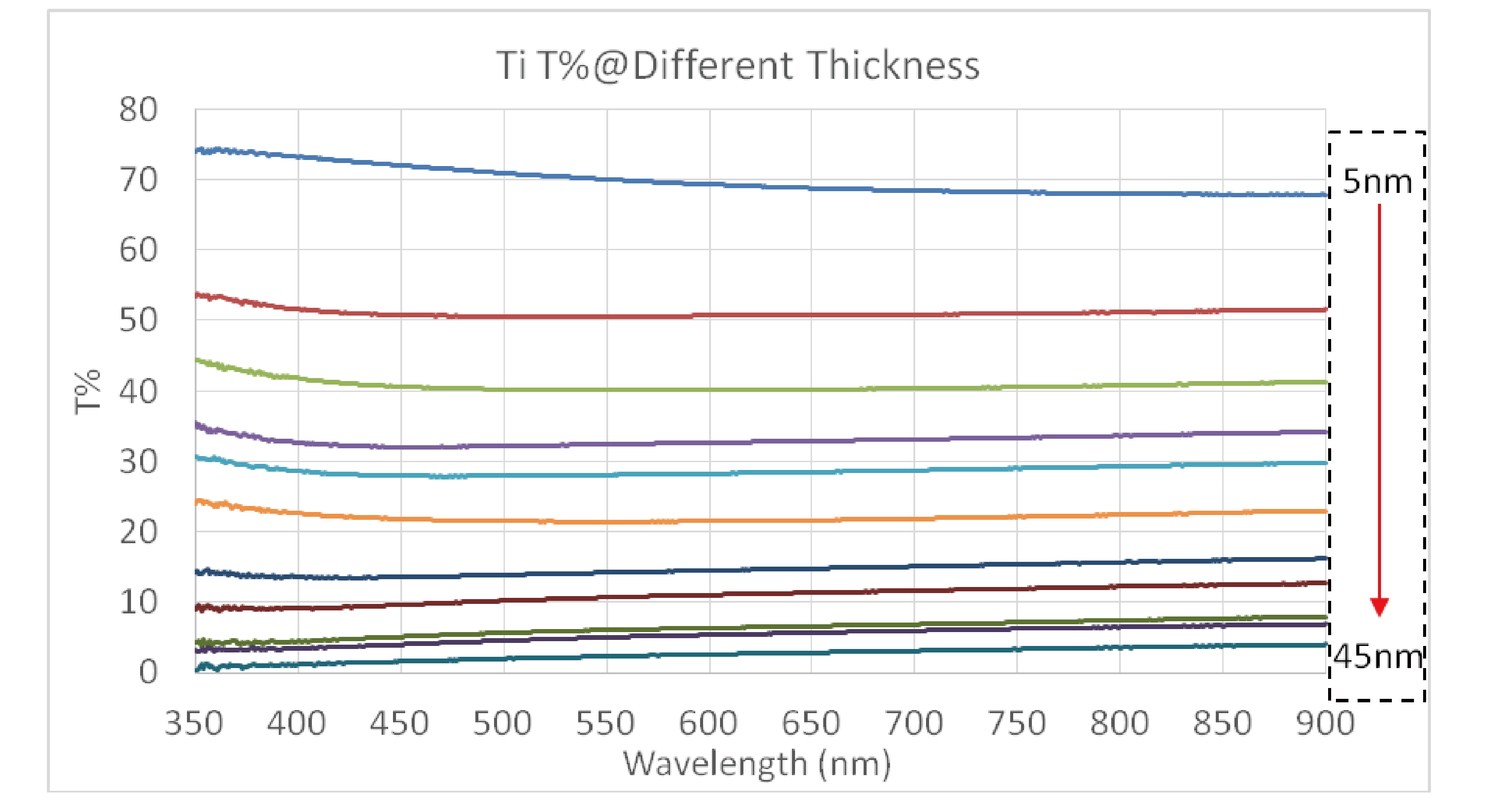
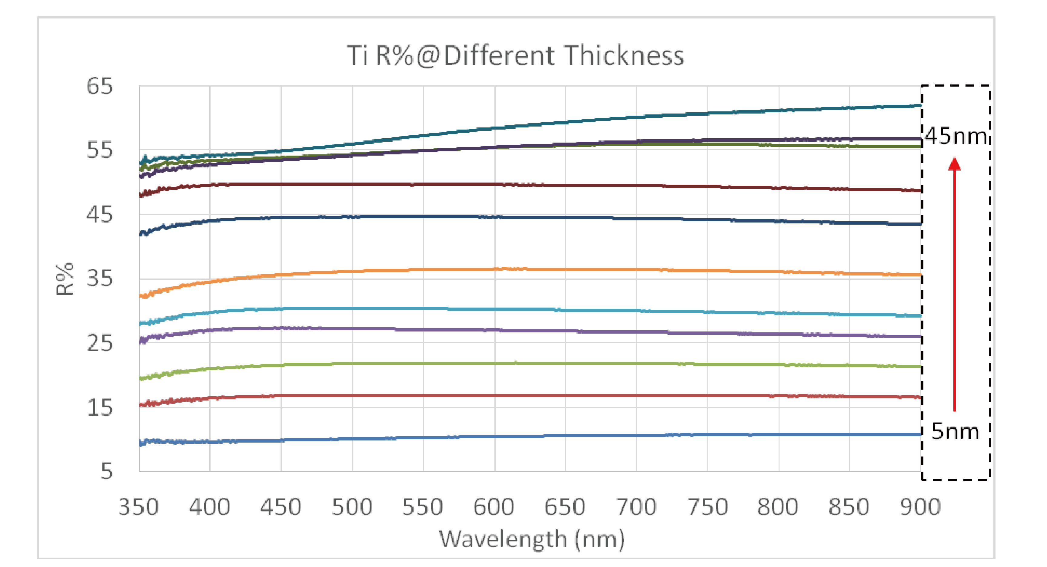
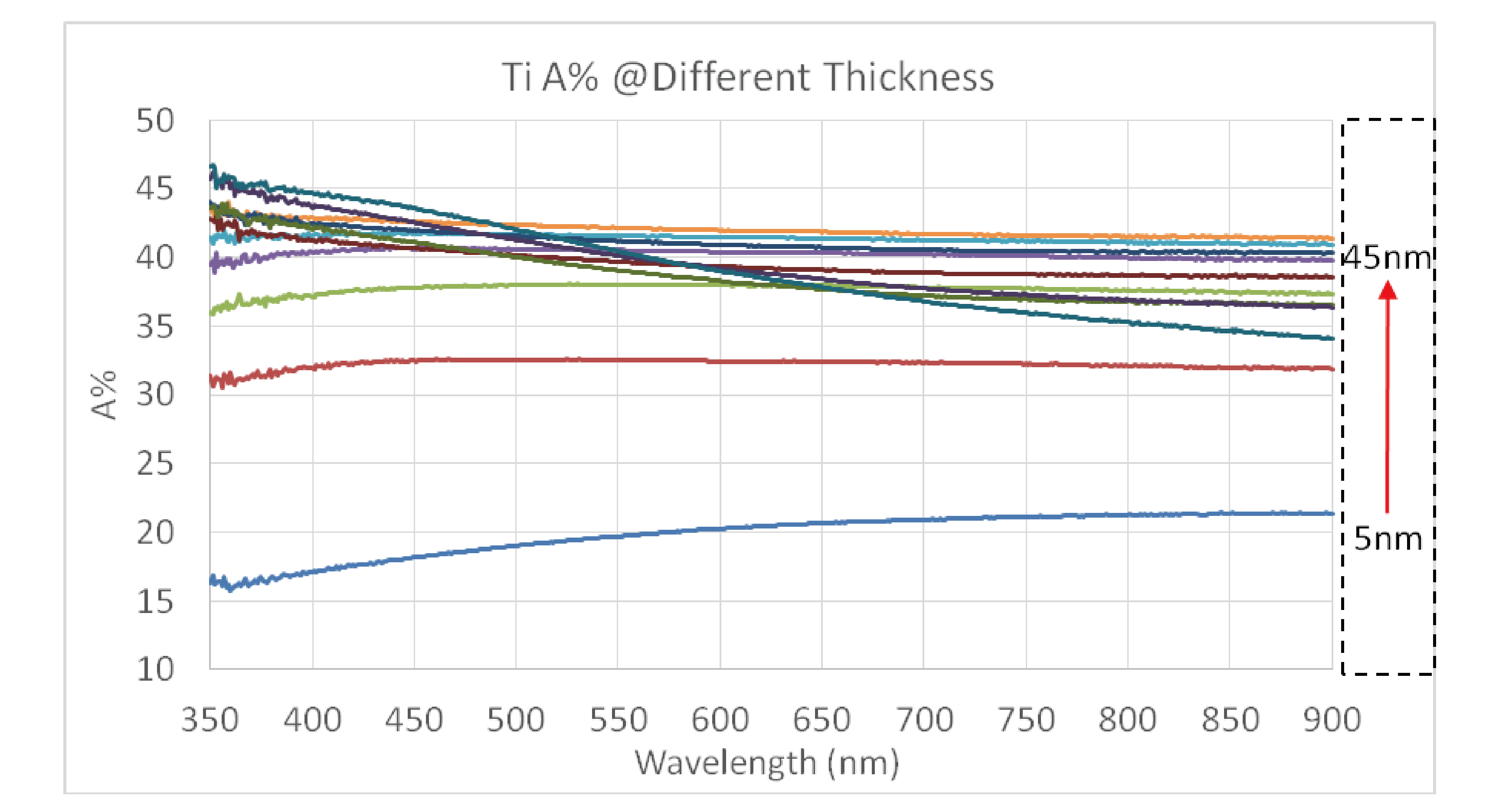
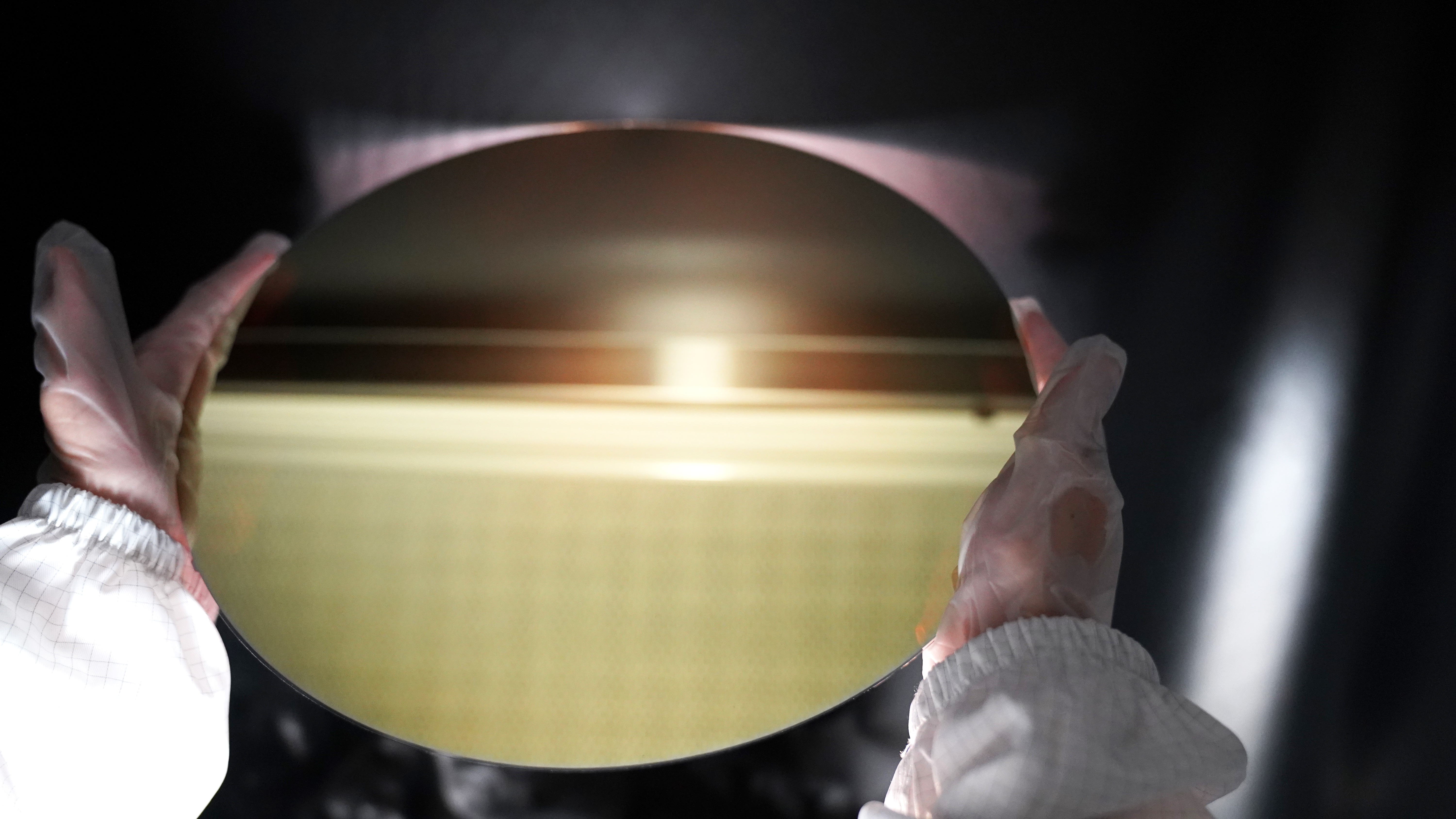
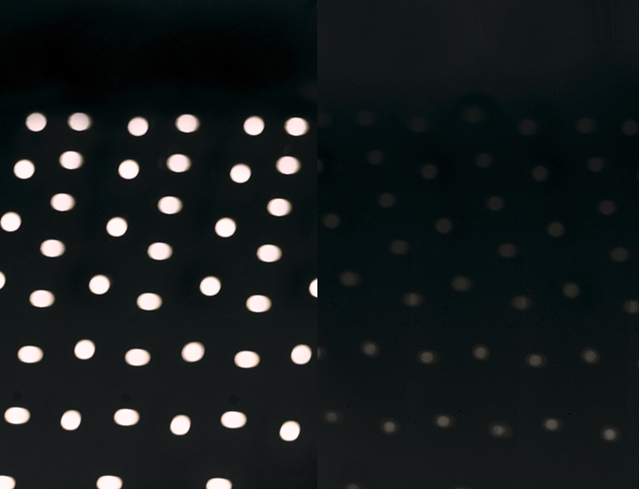
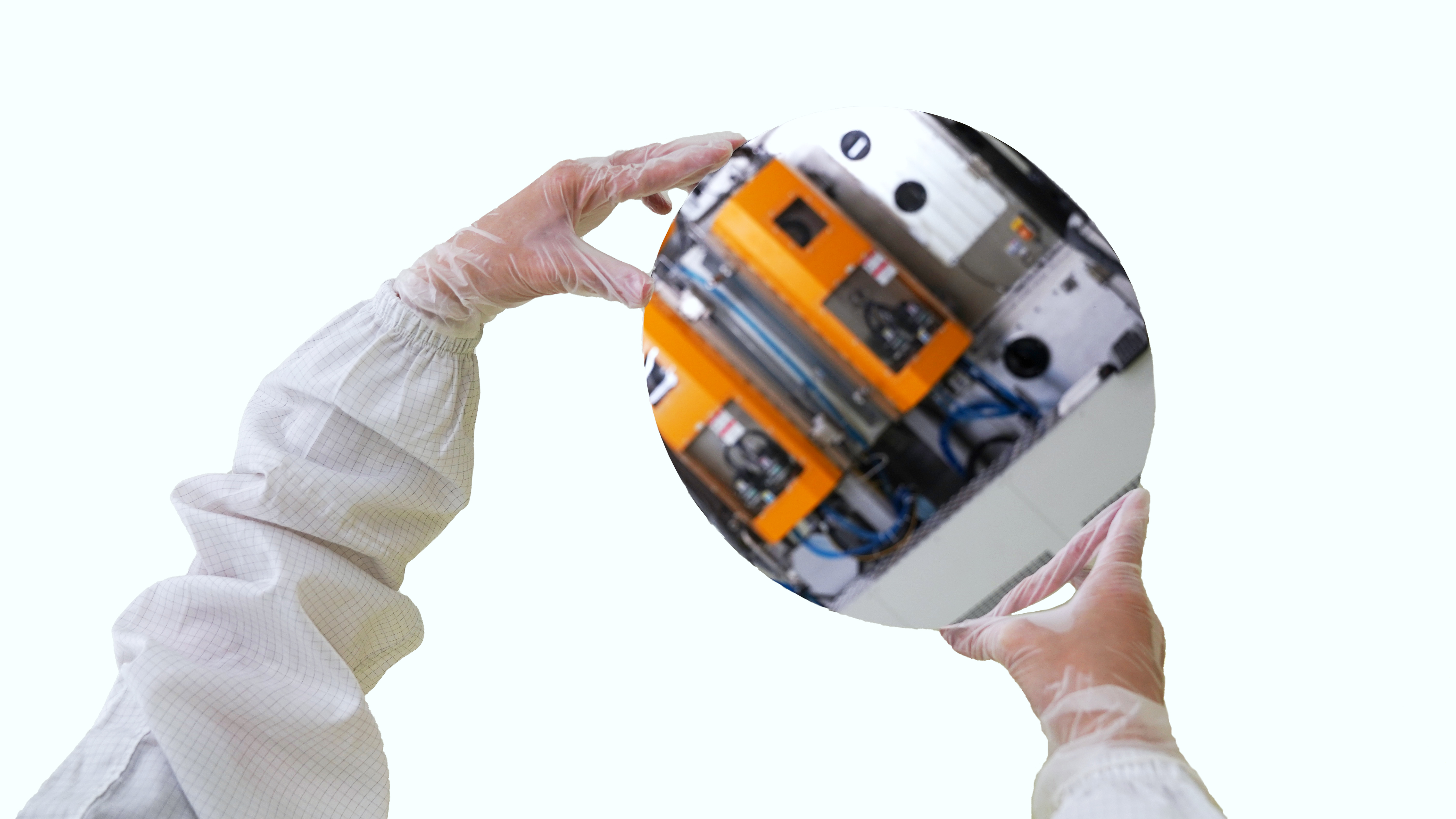
Metal film
Plating Ti, Al, Cu, Sn and other single-layer, double-layer or multi-layer metal films on silicon wafers and regenerated wafers. The thicker metal film is used for electrical conduction and heat conduction, and the thinner metal film can be used for diffusion barrier, For the bonding layer, in addition to silicon wafers, glass and flexible substrates can also be used. The product can be directly integrated into the production line of the semiconductor factory/packaging factory.
GCSOL can quickly provide customized production for various applications through its own optical design and manufacturing platform.
It only needs to put forward the target specifications or requirements, and can quickly simulate, sample and modify according to customer feedback. In the mass production stage, Strict quality management system protects the rights and interests of customers.
GCSOL focuses on optical design and coating foundry.
The development process attaches great importance to customer confidentiality, and it does not involve terminal component products that compete with customers.
GCSOL can quickly provide customized production for various applications through its own optical design and manufacturing platform. It only needs to put forward the target specifications or requirements, and can quickly simulate, sample and modify according to customer feedback.
In the mass production stage, Strict quality management system protects the rights and interests of customers.
GCSOL focuses on optical design and coating foundry. The development process attaches great importance to customer confidentiality, and it does not involve terminal component products that compete with customers.


 Swipe the table right
| Use band range | VIS / UV-VIS-NIR | surface quality | 10/5 (MIL-PRF-13830B) or Semi level |
|---|---|---|---|
| Application field | CIS, Lens, AR/VR, Automotive | Marginal zone | ≦2mm |
| Substrate material | Glass, Si or else | warping | <1mm |
| Substrate range (round) | ≦Φ300mm | Adhesion (Bag test) | Pass ISO Class#0 & ASTM Class#5B |
| Substrate range (square) | ≦350*350 mm | hardness | JISK5600, Pencil: >=9H, Weight: 750g |
| Substrate Thickness Range | 0.1~1.1mm | reliability test | 85℃ 85% : ≧1000 / 1500 hr |