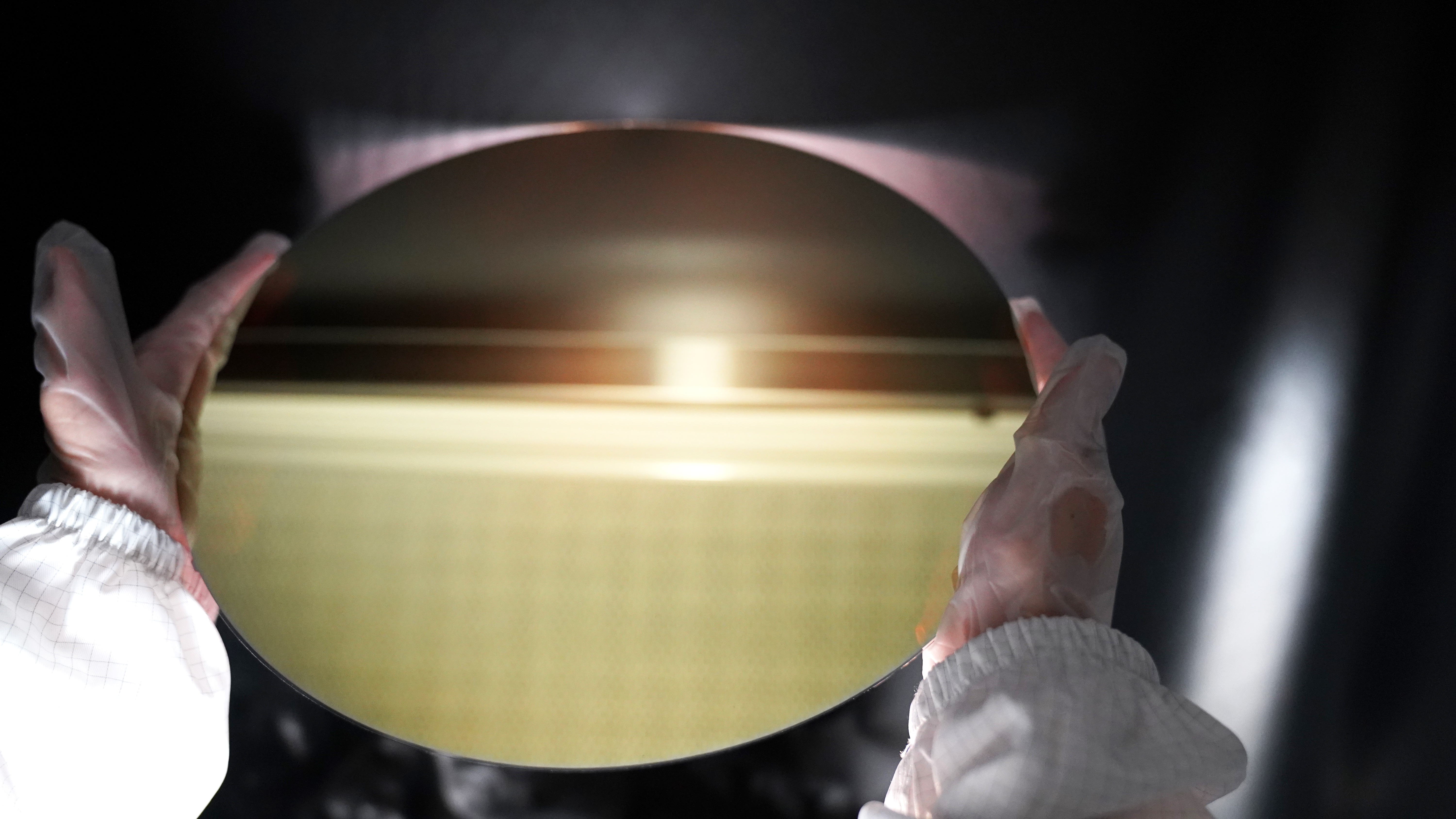
Transparent Conductive Film-ITO
ITO transparent conductive film has good conductivity and visible light transmittance, and can be used as a transparent electrode in various fields, such as photoelectric detectors, displays, solar cells, touch modules, antistatic, electromagnetic wave protection, etc., GCSOL With a variety of ITO process conditions, it is possible to prepare high-quality ITO films at a wide range of process temperatures (RT~400°C), and to apply thin (≧0.3mm) and large-size substrates (≦12"), or those that are not resistant to high temperatures Flexible substrate.
Products can be directly integrated into optical lens assembly/semiconductor packaging production lines, such as WLP (Wafer level package).
It can be combined with patterning, dicing process or other functional films, such as anti-reflection film (GC-BBAR), filter film (Filter), black film (Black Matrix), etc., to better improve device performance.
IMITO (Index matching ITO) planning can be customized to greatly improve the transmittance and improve the optical characteristics of the product under the premise of achieving electrical properties.
Wafer-level optical coatings can be provided: the product surface quality of the semiconductor mature process level, and the ability to resist chemical cleaning is enhanced.
GCSOL can quickly provide customized production for various applications through its own optical design and manufacturing platform. It only needs to put forward the target specifications or requirements, and can quickly simulate, sample and modify according to customer feedback. In the mass production stage, Strict quality management system protects the rights and interests of customers.
GCSOL focuses on optical design and coating foundry. The development process attaches great importance to customer confidentiality, and it does not involve terminal component products that compete with customers.


 Swipe the table right
| Use band range | VIS / NIR | surface quality | 10/5 (MIL-PRF-13830B) or Semi level |
|---|---|---|---|
| Application field | CIS, AR/VR, LCD | Marginal zone | ≦2mm |
| Substrate material | Glass, Si or else | warping | <1mm |
| Substrate range (round) | ≦Φ300mm | Adhesion (Bag test) | Pass ISO Class#0 & ASTM Class#5B |
| Substrate range (square) | ≦350*350 mm | hardness | JISK5600, Pencil: ≧9H, Weight: 750g |
| Substrate Thickness Range | 0.3~1.1mm | reliability test | 85℃ 85% : ≧1000 / 1500 hr |